Key Takeaways
- PCBs are critical to electronic device performance, and even minor defects can cause device failure or safety risks.
- Common PCB defects include short circuits, open circuits, poor solder joints, and component misplacement, all of which impact reliability and production yield.
- Testing methods like Automated Optical Inspection (AOI), X-ray inspection, In-Circuit Testing (ICT), and functional testing identify defects at every stage of production.
- Rigorous PCB testing reduces rework, scrap, recalls, and warranty claims, ultimately saving costs and protecting brand reputation.
- Comprehensive testing ensures compliance with industry standards, enhances reliability, and supports long-term customer satisfaction.
Introduction
Printed Circuit Boards (PCBs) drive the functionality of nearly every modern electronic device. As such essential components, ensuring their quality directly impacts the performance and safety of everything from consumer gadgets to industrial control systems. A single oversight, such as an unnoticed defect, can cause devices to malfunction or fail altogether. To guard against these risks, manufacturers pursue rigorous testing protocols at each step of the production process. Whether working with a large assembly line or a custom PCB design company Santa Clara, CA, comprehensive testing is the foundation of reliable electronics.
The scrutiny applied during PCB manufacturing not only safeguards the integrity of the end product but also protects companies from costly recalls and reputational harm. In high-stakes markets, attention to quality is non-negotiable. Test strategies are tailored to address common defects encountered during fabrication and assembly, leveraging specialized technologies and standardized methods to achieve optimal results. Reliable PCBs are the backbone of modern electronics and demand a diligent approach to quality assurance.
Common PCB Defects and Their Implications
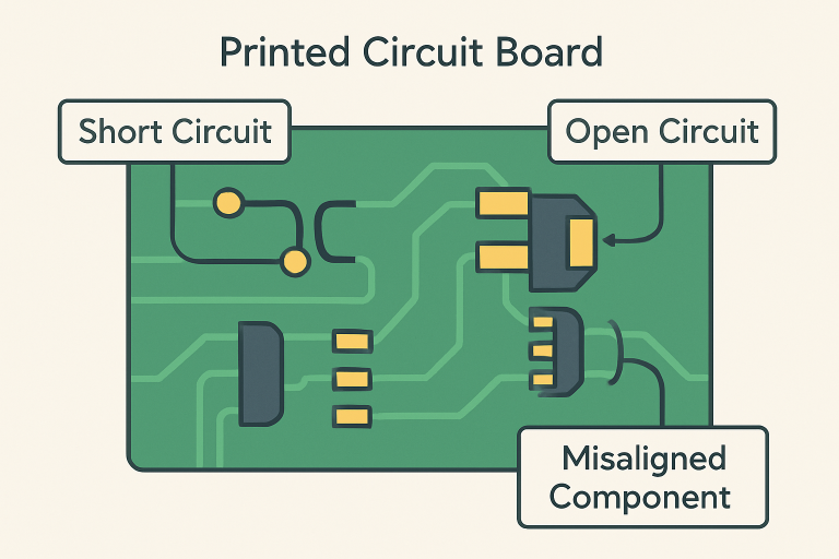
Defects in PCB manufacturing can vary in their causes and consequences. The most frequent issues include:
- Short Circuits: Unintended connections between conductive traces can lead to overheating and device shutdowns.
- Open Circuits: Breaks in pathways prevent the electrical current from reaching its destination, leading to non-functionality.
- Poor Solder Joints: Weak or incomplete soldering can cause intermittent faults and gradual device degradation.
- Component Misplacement: Incorrectly placed electronic elements result in compromised performance or complete failure.
These defects have far-reaching implications. Device reliability drops, production yields decrease, and the risk of post-market failures that could endanger users or disrupt services grows. For consumer-facing companies, recurring problems can cause lasting brand damage and prompt stricter scrutiny from regulatory bodies. In industries with strict standards, such as automotive or medical devices, even a minor error can have significant safety or financial ramifications.
Key Testing Methods in PCB Manufacturing
Successfully identifying and addressing PCB defects requires an array of testing techniques. Manufacturers rely on various complementary methods to ensure thorough evaluation and validation at each phase of assembly and after the board is complete.
Automated Optical Inspection (AOI)
AOI offers a swift, non-invasive method for checking PCBs for visible defects. Using high-resolution cameras and pattern recognition software, AOI systems scan assembled boards for missing, skewed, or misaligned components, as well as soldering and surface flaws. The ability to conduct this inspection at multiple process stages helps manufacturers minimize rework and waste, ensuring only boards free of obvious defects move on to the next steps of production. According to EE Times, AOI’s efficiency makes it a go-to solution in high-volume manufacturing environments.
X-Ray Inspection
For multilayer or densely populated PCBs, visual inspection alone is inadequate. X-ray inspection penetrates the board, revealing otherwise hidden issues like internal short circuits, voids in solder joints, or insufficient solder beneath BGAs and CSPs. The in-depth analysis provided by X-ray technology uncovers subtle flaws often missed by other means, supporting higher manufacturing yields and heightened product safety, especially for complex, mission-critical boards.
In-Circuit Testing (ICT)
ICT is among the most robust tools for ensuring PCB functionality at the component level. By using electrically conductive probes, ICT checks for shorts, opens, and incorrect component placement while also validating resistance, capacitance, and functionality where accessible. This method is favored for its scalability, speed, and ability to detect faults that could hinder board operation once deployed.
Functional Testing
Functional testing represents the final quality gate before boards are integrated into finished products. Unlike previous methods, functional testing validates the board’s behavior under actual operating conditions. The PCB is energized and made to perform the tasks for which it was designed, verifying that all features respond correctly under both normal and stressful environments. This form of testing ensures not just assembly accuracy but also that each board achieves its intended purpose once deployed.
Benefits of Rigorous PCB Testing
Exhaustive testing is both a quality and a business imperative. Key benefits include:
- Early Defect Detection: Problems are identified before they progress down the line, reducing the rates of rework, scrap, and field failures.
- Cost Savings: Efficient test processes prevent defective boards from reaching customers, avoiding large-scale recalls, warranty claims, and potential litigation.
- Enhanced Reliability: Quality controls ensure equipment performs as intended for its full lifecycle, pleasing customers and building trust in your brand.
- Compliance with Standards: Rigorous testing is essential to demonstrate conformance with global safety and industry-specific performance standards.
Final Thoughts
As innovation pushes electronics into new markets and applications, the importance of reliable PCB testing has never been greater. Consistent application of inspection and validation techniques such as AOI, X-ray inspection, ICT, and functional testing empowers manufacturers to uphold quality, reduce costs, and meet or exceed industry standards. These measures transform PCB testing from a checklist item into a central pillar of successful electronics manufacturing. By investing in comprehensive testing protocols, businesses ensure long-term device reliability and foster lasting customer satisfaction.